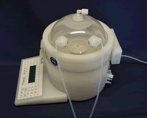
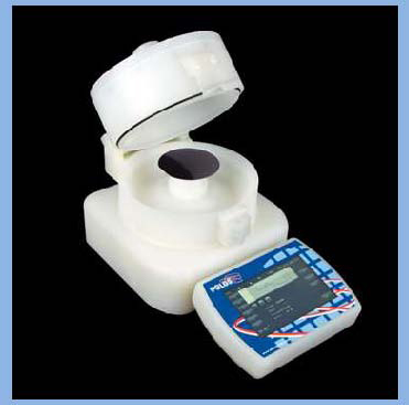
 APT spin200
 |
|
- Ideal for Process R&D
- Material Size: Ø8”Wafer or 6”square Glass
- RPM: 1 ~12.000 rpm : 300RPM 이하의 저속 제어가능
(for mechanical/non-vacuumchuckswe recommend max. 3.000rpm)
- Program:무한 프로그램, 무한 스텝 가능
- Accuracy (+/-0.1 rpm),Digital control Stepping Motor
- Chemical resistant NPP or Teflon Bowl
- Digital Process Controller-easy step-by-step
- Acceleration/Deacceleration max:30,000 rpm/sec
- Clear Lid with 19mm center hole
- Drain Port, Nitrogen Purge Port
- Specially designed Bowl for Anti-Reflection & Reducing
the the airflow to zero
- Safety Door Interlock:Rotating stops when opening door
- Centering Tool Included
- German-APT Made CE-approved
- Remote control pannel available (Globebox 사용시 유용)
- chuck :Fragment ,6-8''wafer
- 용도 : 웨이퍼 PR 코팅,유기박막코팅,
ITO Glass 박막코팅
작동 모습
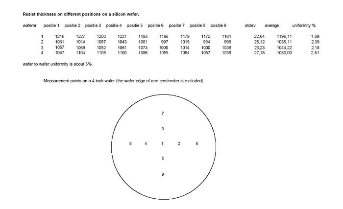
Determination of spincoating uniformity and wafer to wafer uniformity
of the APT Spincoating system using AZ5214E resist.
( By: T. Zijlstra TUDelft B. de Lange TUDelft B. van Weelde SPS )
- APT Spincoater의 특징
Wafer uniformity의 향상을 위한 2 Point
1. acceleration during ramp up: Changing the acceleration
resulted in more smooth resist films,
i.e. “comet” tails disappeared when the acceleration
during ramp up was increased to 1000 rpm per second, with a final spinning
speed of 5000 rpm.
2. Airflow in the spinbowl: Reducing
the the airflow to zero resulted in circular uniformal resist
pattern on the wafer
- Wafer to wafer uniformity:
** For these experiments we used the “optimized” conditions,
i.e. a ramp up of 1000 rpm per second for five seconds, then a spinning
speed of 5000 rpm for 55 seconds.
The airflow in the spinning bowl was reduced to zero.
1. The spinning conditions for AZ 5214E was optimized, although we are
convinced that conditions could have been further optimized if we would
have had more time available.
2. The wafer uniformity found, is better than 2.5%
3. The wafer to wafer uniformity was found to be 3%.
4. Improving the experimental setup would probably resulted in better
wafer uniformity and wafer to wafer uniformity.
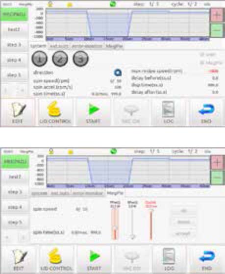
키보드 프로그램 과정

|
 Spincoater
Home
 Spincoater
Home
 APT spin200